Sunday, May 10, 2015

practical 'ow 'er logic test

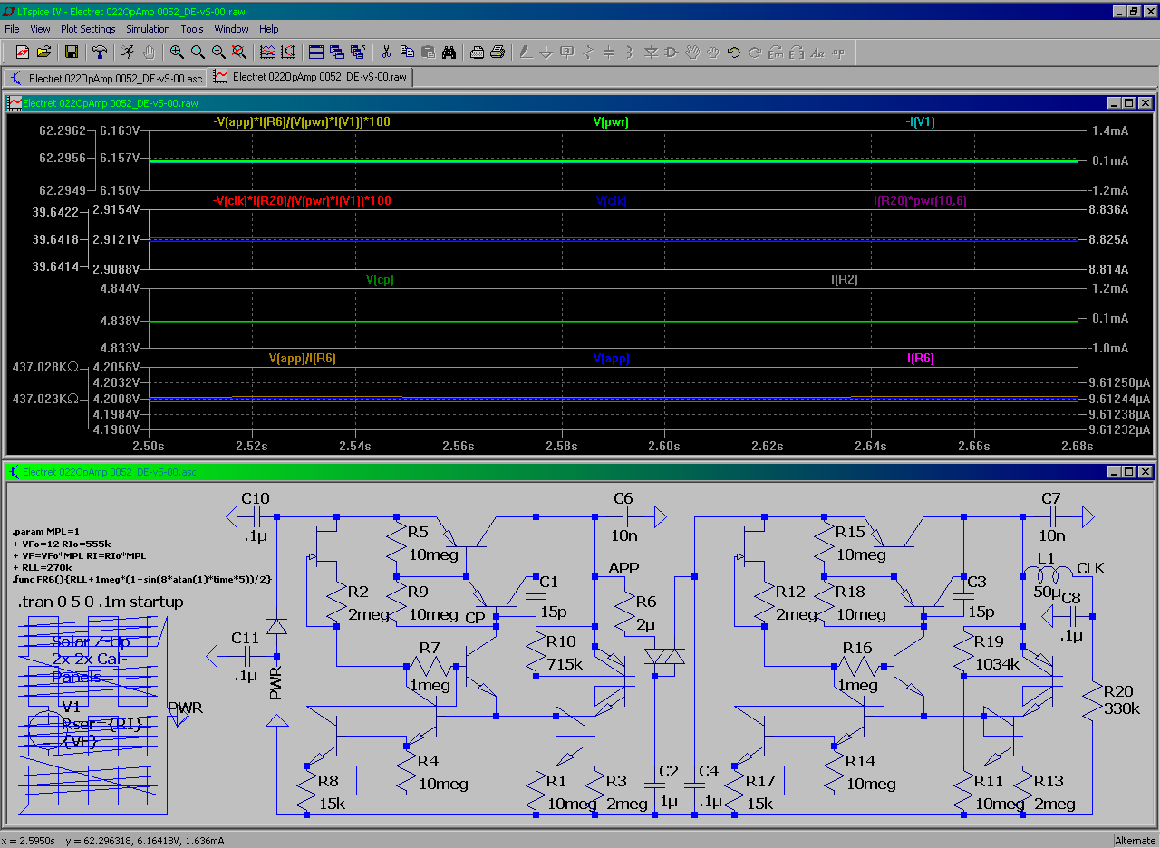
needed a 1:10 duty oscillator - so i revised/-studied/-tested some trivial generator types . . . the schmitt-inverter showed up a fairly good properties for design target (power levels indication) - more over the inverter passed the basic logic test without any modifications (this is like something extraordinary)


and the schmitt+inverter itself with SB captured 2-ch scope diagram through 1nF+3.6kΩ decoupler-probes

if you remove the 15pF capacitor and add input diode pairs you'll have a set of 7µA NAND-s

Sunday, April 19, 2015

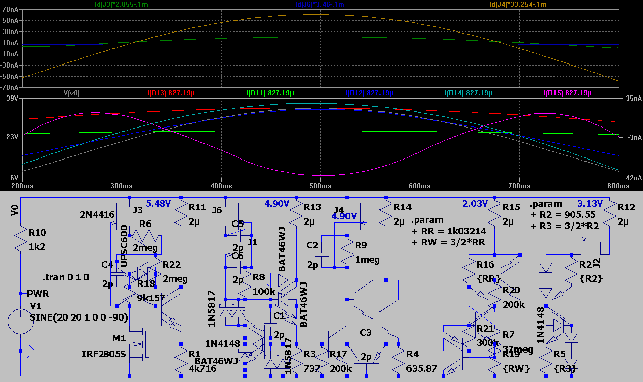
Simple Current Limits Compared (Updated!)

Type.1

Type.2

Update !!!
► emerged by the predecessor of the second from the right - a "constant current shunt" - that was the best performing such in one of the experimental linear regulators (now revisited)see also :: yet another constant current source

Friday, April 17, 2015

Regulator Redesign (/Lab -- as always . . .)

________________________________________________
2015-04-15 ::
¯¯¯¯¯¯¯¯¯¯¯¯¯¯¯¯¯¯¯¯¯¯¯¯¯¯¯¯¯¯¯¯¯¯¯¯¯¯¯¯¯¯¯¯¯¯¯¯
 . . . trying to "de(/un)-bug" the last design from prev. post -- normalize power range , minimize the error . . .

+ a modified v.'s foldback diagram


Customizing/"improving" the 78Lxx for 1.2V

i only guess it's 3.0V
________________________________________________
2015-04-16 ::
¯¯¯¯¯¯¯¯¯¯¯¯¯¯¯¯¯¯¯¯¯¯¯¯¯¯¯¯¯¯¯¯¯¯¯¯¯¯¯¯¯¯¯¯¯¯¯¯
"Minimizing Compile" , exploring the switcher mode v. , experimenting with foldback . . .

thought to use the LT's µ-P 2.5V LDO -- but the 3uA is likely causing it's instability in high loads env.


________________________________________________
2015-04-17 ::
¯¯¯¯¯¯¯¯¯¯¯¯¯¯¯¯¯¯¯¯¯¯¯¯¯¯¯¯¯¯¯¯¯¯¯¯¯¯¯¯¯¯¯¯¯¯¯¯
Optimizing "Design"

Update! :: the foldback re-visited . . .
Update+ :: ±10µV version ::
Update+ :: ±12µV version with foldback updated to support high load capacities (no frequency test - what so ever- carried out + i donno how to thermal compensate - /!\ so i never do /!\) e.g. you have to recalculate the design before any attempt to assemble it

________________________________________________
[EoP]
¯¯¯¯¯¯¯¯¯¯¯¯¯¯¯¯¯¯¯¯¯¯¯¯¯¯¯¯¯¯¯¯¯¯¯¯¯¯¯¯¯¯¯¯¯¯¯¯

Saturday, April 11, 2015

a low control current capable voltage regulator

Here's the grid - simulated fine (actually excellent -- that's why the design's revisited . . .) in prev. (a non TEST) v. but it didn't regulate "at all" in a real build -- here "we" possibly identified why -- if the R1 is too high (too little load) the VZ may go high thus also VT climbs out of the range and - bam! - we have a multiples of higher voltage on output than it's expected (the RED outlines the voltage regulation logic) ::
Next - omitting the CC module + startup chain - simplifies the design but we loss a magnitude of precision ::
Here follows a very poor example of a step-dn swithing regulator - asctually i didn't preserve the original v. of it (this is a fast feature restoration) coz i could not clear/filter the unwanted ringing and simulates extreamly slow . . . however the feature is a "built in" PPM (a pulse position modulation) capability (extra to low control current capability) -- needs a lot more testing to get it near right . . . (notice the varying supply internal resistance -- is why the efficiency graph wont link up exactly) ::
Omitting the VT reference point results in additional precision loss . . . but it revealed some specific behaviours of this type of regulation scheme (some of which're mentioned on o figure) ::
Here we've a near max low control current scheme - it starts auto-limit it's output current (depending on input supply) @ 150...200mA (output current max 235mA -- SC current 238mA) . . . and it seems to use some 110µA for regulation . . .
. . . a big deal considering the Solar battery test design with avg. 10.5µA TOT.supply draw - 8.8µA load current = 1.7µA (16%) regulation current . . . ::
. . . while the "near max low" v. ↑↑ has 108uA / 18mA avg. = 0.59% ( 120µA / 83mA peak = 0.15%) regulation currents

Sunday, April 5, 2015

Adjusting the adjustable voltage regulator

The goal as in trivia is to gain more stability and precision while keeping the design robust . . .


9V ± 1.8µV , 300/646mA (max.load/SC.supply current)
-- the stability (ringing(OpAmp-s e.c.)) + SC condition are a question marks here


((Simple with SC don't care /!\)) 9V + 0.6 ± 2.6mV , 300/687mA


((Simple SIPMOS with SC handling)) 9V + 4 ± 475 µV , 300/687mA


((BJT alternate of the above)) 9V - 48 ± 255.6µV , 300/56.7(398)mA (max.load/SC.supply current.average(.peak))


((feature test for FET switching)) 9V - 7 ± 13mV , 346/706(CuLm+)mA , 23.7kHz (here for err. compare)
-- the main targets were the inductor&frequency versus load&error (the current limit is a quick fit -- feature test)

[EoP] (XT kogu aeg on mingi vitustus selle küljendamisega -- ma korjan mittevajalikud reavahed maha - aga voila! - peale save´imist on nad kuskilt tagasi tekkinud (teksti ja pildi vahele topitakse <BR> tag´id - et kui on huvi lõpmatuseni oma tekstiga jantida ÕööÖרÛÜÚÝ♒☣☠☦☯ ))